
Semiconductor lithography is where engineering meets nanotechnology—a realm where precision isn’t measured in millimeters, but in nanometers. Behind the scenes of every cutting-edge chip fabrication process lies a marvel of mechanical design: the lithography tool. These machines, responsible for etching microscopic patterns onto wafers, demand mechanical tolerances tighter than a human hair’s width. As a mechanical engineer working on semiconductor system development, I’ve seen firsthand how multi-physics simulation and mechatronics integration drive the performance, stability, and throughput of these machines.
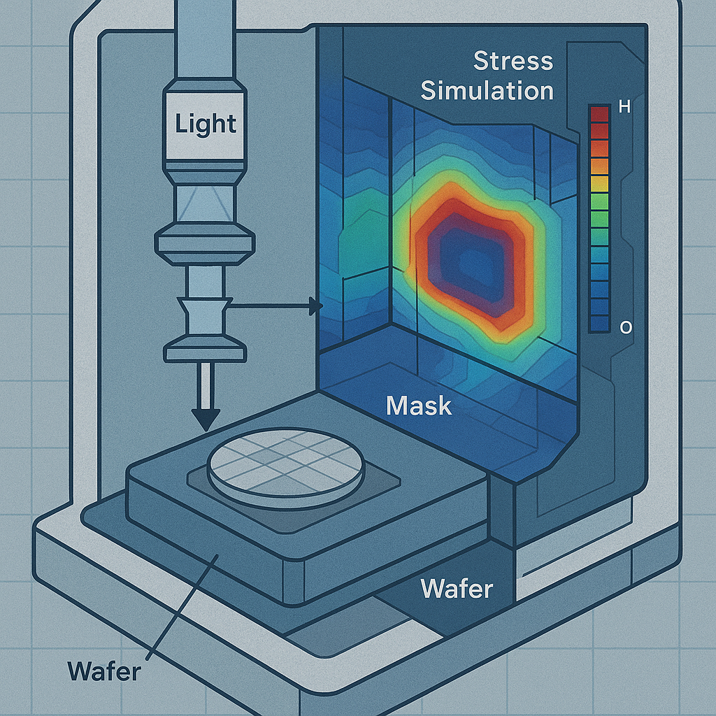
Unlike conventional industrial equipment, lithography platforms are hybrid systems—merging optics, robotics, thermal systems, and vibration-dampened stages into a single synchronized operation. Even minor misalignments due to thermal expansion or stage drift can destroy an entire batch of wafers. That’s why finite element analysis (FEA), coupled with computational fluid dynamics (CFD), plays a central role in design and prototyping. These simulations model heat transfer, mechanical deformation, and flow behavior inside components like lens housings, vacuum chambers, and actuator arrays—ensuring that every part behaves as expected under dynamic stress.
One of the most critical mechanical subsystems is the wafer stage—a high-speed platform that positions wafers with sub-nanometer accuracy. It must resist vibration, absorb thermal load, and respond to control feedback in real time. Achieving this level of control requires not only simulation-backed design, but also materials engineering—where thermal expansion coefficients and structural damping properties are carefully matched. In my work, we’ve tested composite materials and applied layered damping to optimize the stiffness-weight ratio for long-term reliability.
Another key consideration is contamination control. Lithography tools operate in ultra-clean environments, where even micro-particles or outgassing from components can lead to defects. Engineers must design parts with low particulate generation, easy cleaning access, and bake-out compatibility. Advanced 3D modeling helps predict where contamination might accumulate—and simulate airflow behavior inside the housing to mitigate it.
Ultimately, precision engineering in lithography isn’t just about building machines—it’s about engineering the invisible. Every adjustment in geometry, material, or cooling flow influences the accuracy with which chips are printed at 5nm and beyond. As we enter the era of EUV lithography and atomic-scale transistors, mechanical engineering must continue evolving with the same precision as the semiconductors it helps create.